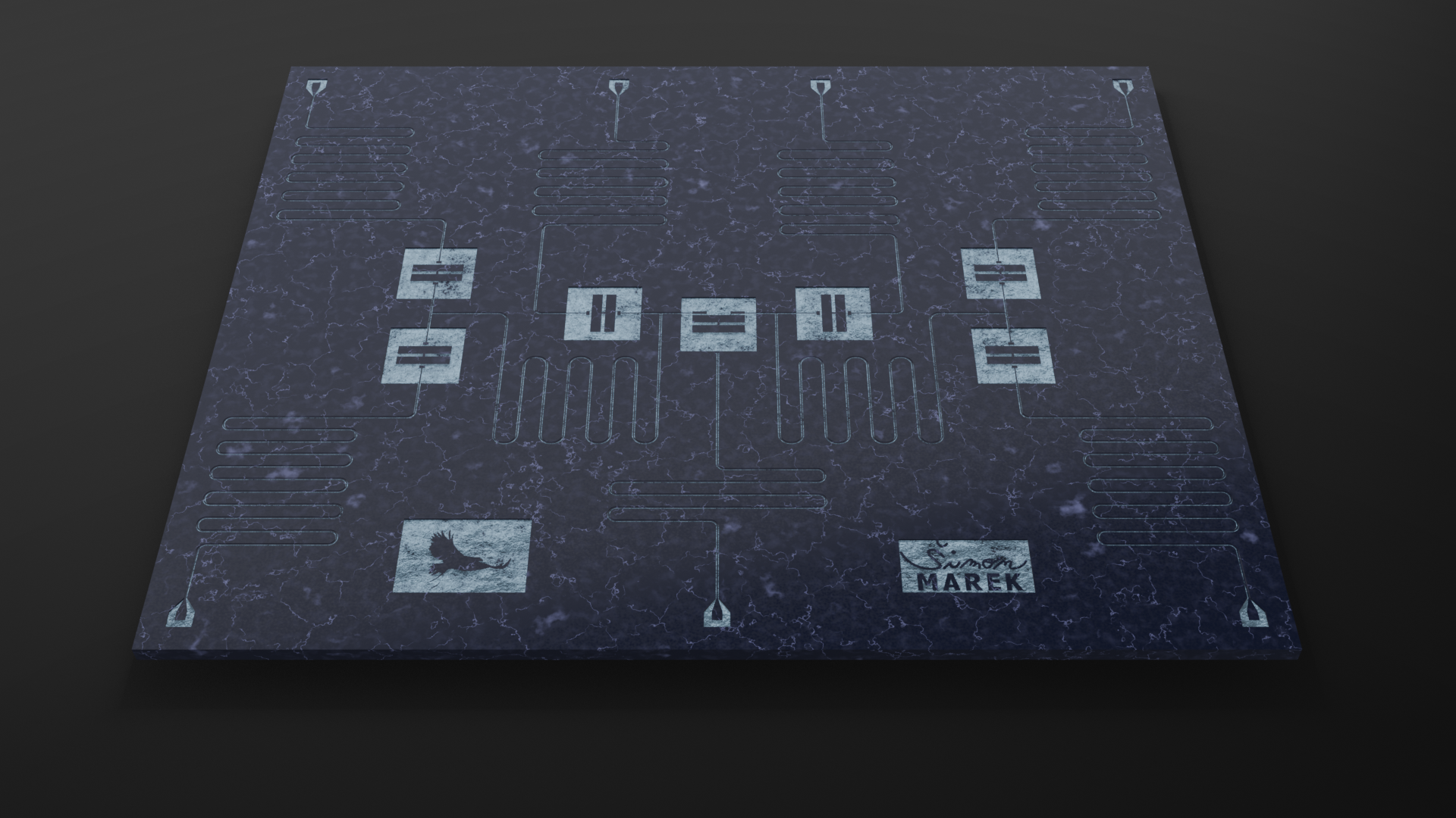
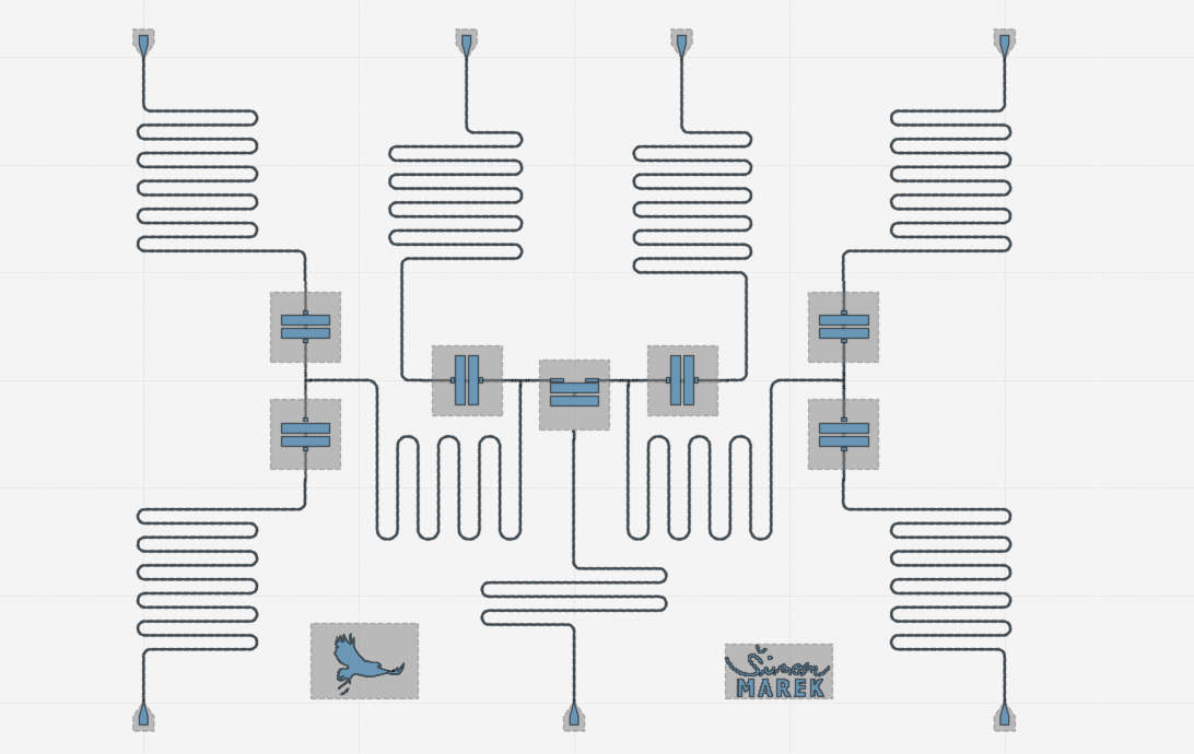
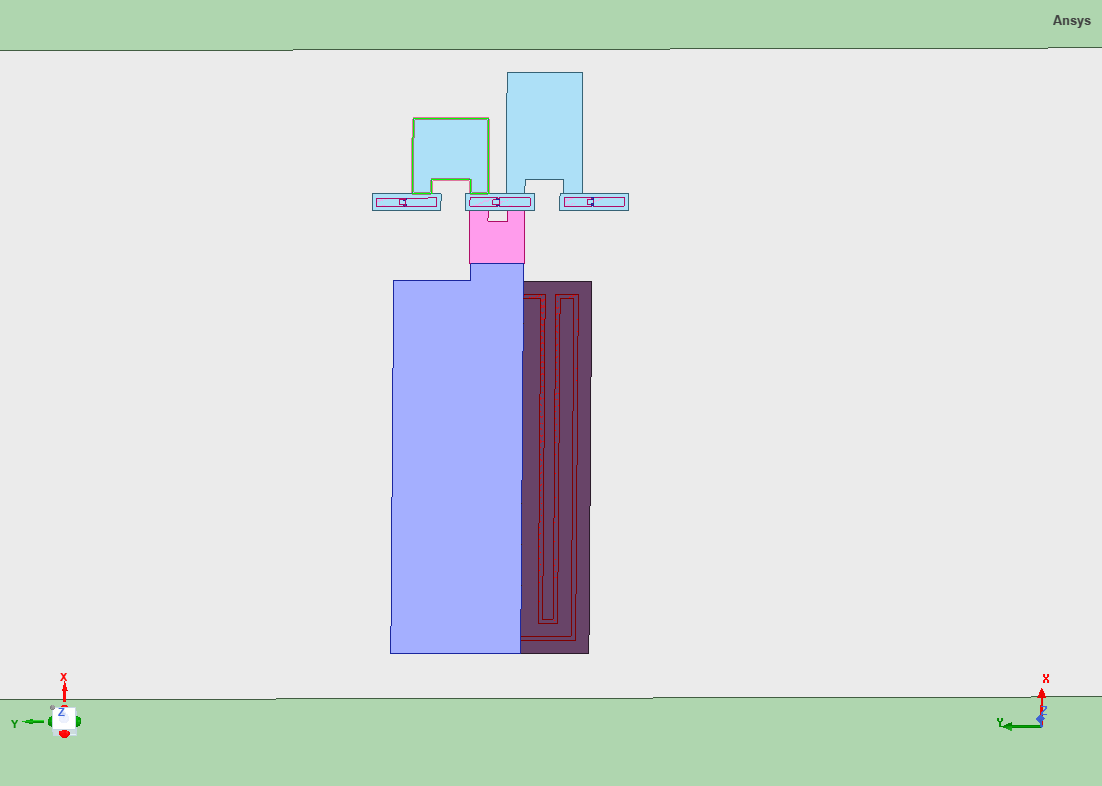
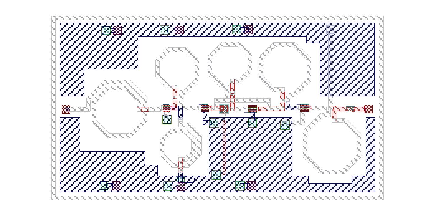
Quantum hardware design, I mostly focus on quantum chip engineering. Main qubit type I use are transmons and starmons. I design quantum chips with full workflow starting from circuit simulation, chip layout, FEM simulation, GDSII preparation and visualisation. I do quantum chips in design themes or series and I do iterations of quantum chip designs
JTWPA Amplifier Design
For Amplifier design I do every type which contains Josephson Junction so, variations of TWPA and JPA. For this type I can prepare Circuit simulation regarding S11 parameters, Impedance profiles Z-parameters, currents for JJ, I use tool with built in model for JJ, for other more specialized types of sims I use Josephson circuits, I can do layout,FEM and GDSII.
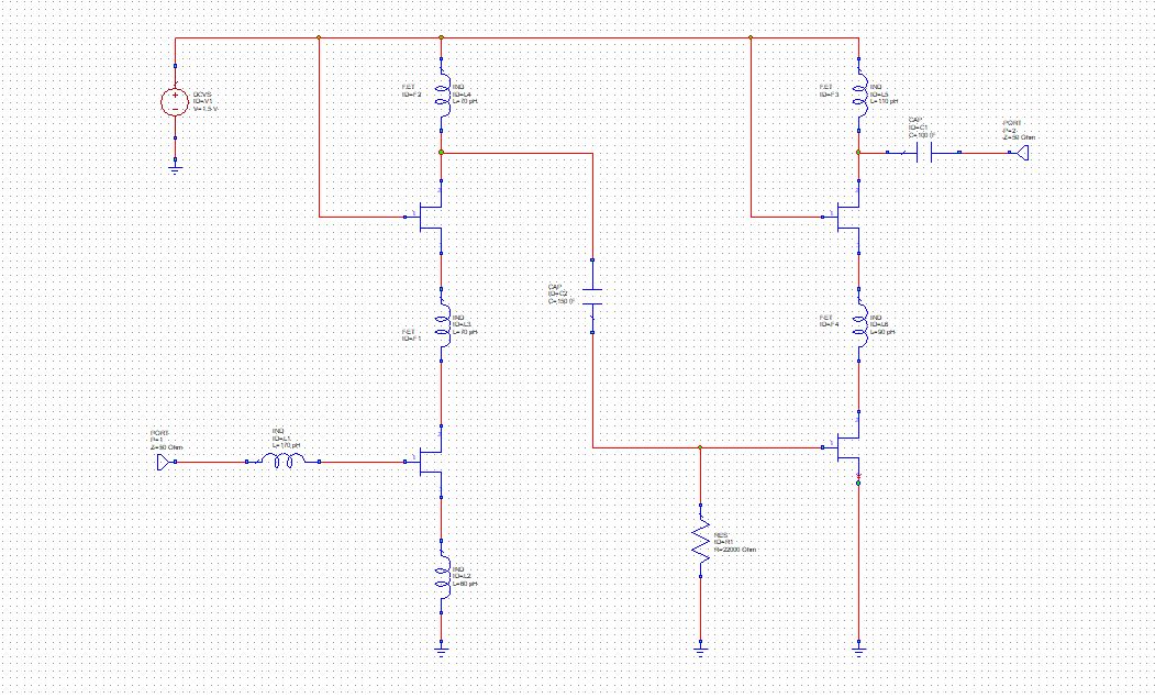
RFIC HEMT Chip Design
Engineering RFIC HEMT – I can do everything from circuit simulation of elements, simulation, characterisation, and modelling of custom on chip inductors. I can do planning of selection of right PDK. Creation of right chip layout! Then exporting it to FEM and evaluating its parameters like electric fields, inductance, capacitance, s parameters. Then creating GDSII and preparing for manufacturing
mmWave & RF Engineering
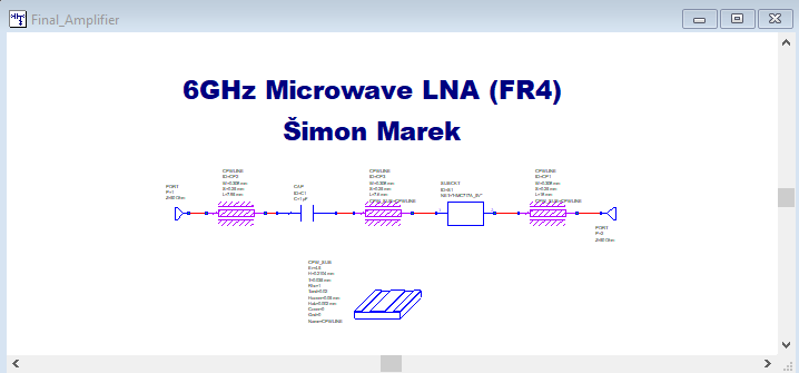
mmWave & RF engineering, I always start with picking proper components, evaluating its models and datasheets, then reading application note. When Im confident with my components I do circuit simulation, then layout, later FEM simulations for some circuits, later validation of gerber files, then manufacturing, inspection, measurement and testing.
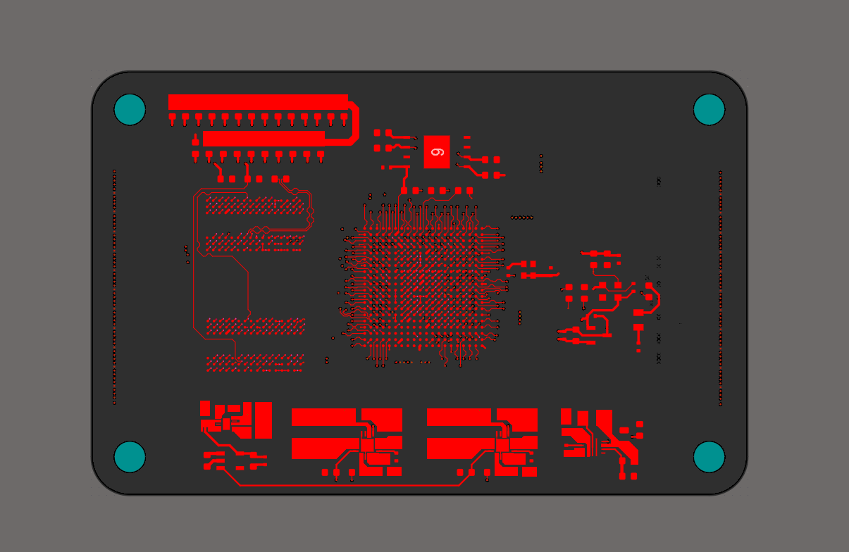
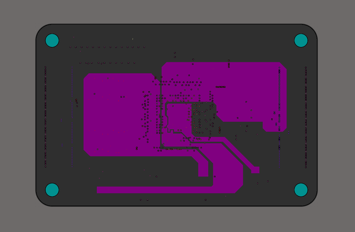
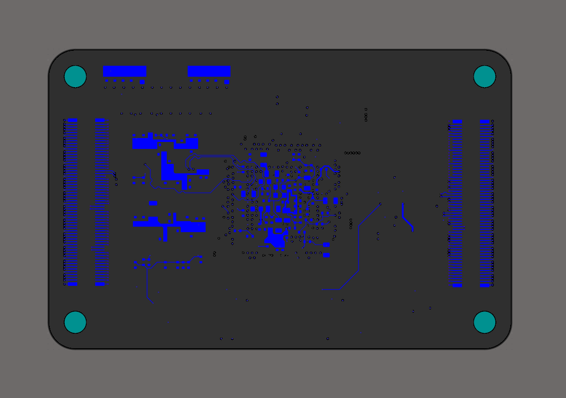
Control Electronics & PCB
PCB design of control electronics boards for quantum computing with FPGAs. I start with selection of components, reading application notes and required circuitry needed to build this design, sometimes I take inspiration from exsisting designs and extract parts I really like to design my new enhanced version. Then I do schematics accordingly and then move to creating layout. Then I send it manufacturing and do testing.
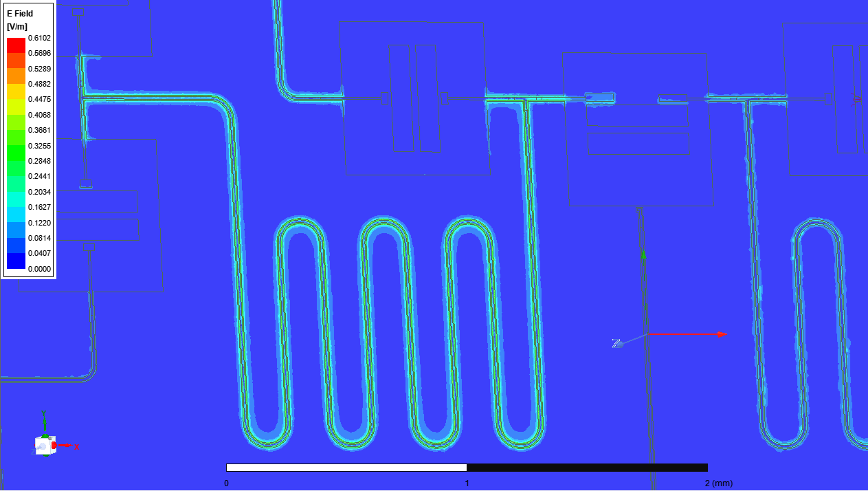
FEM & Circuit Simulations
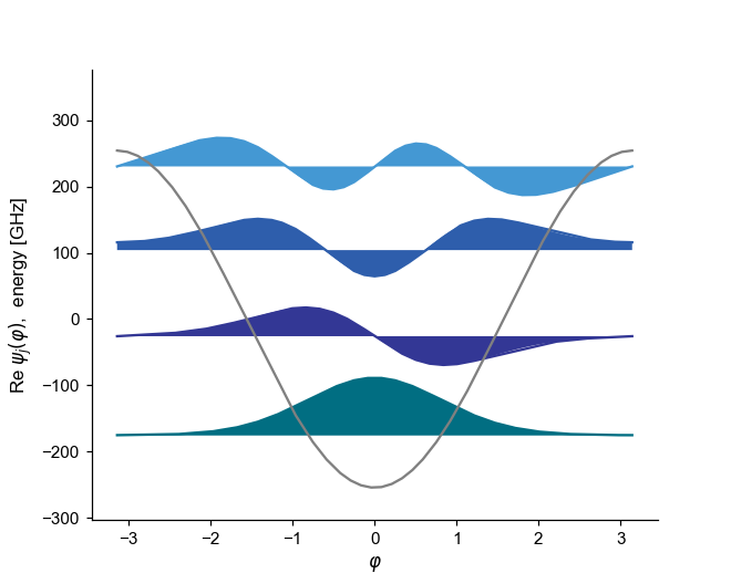
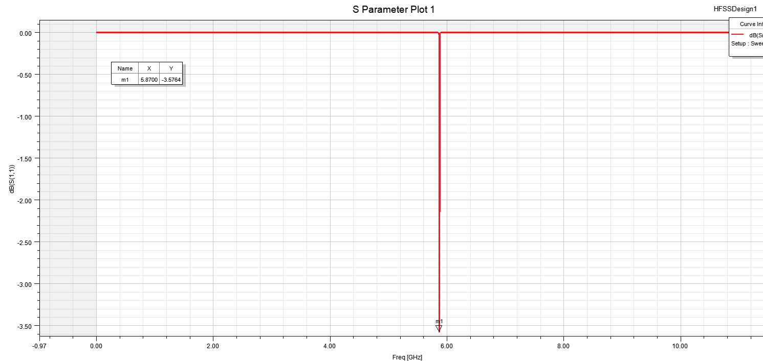
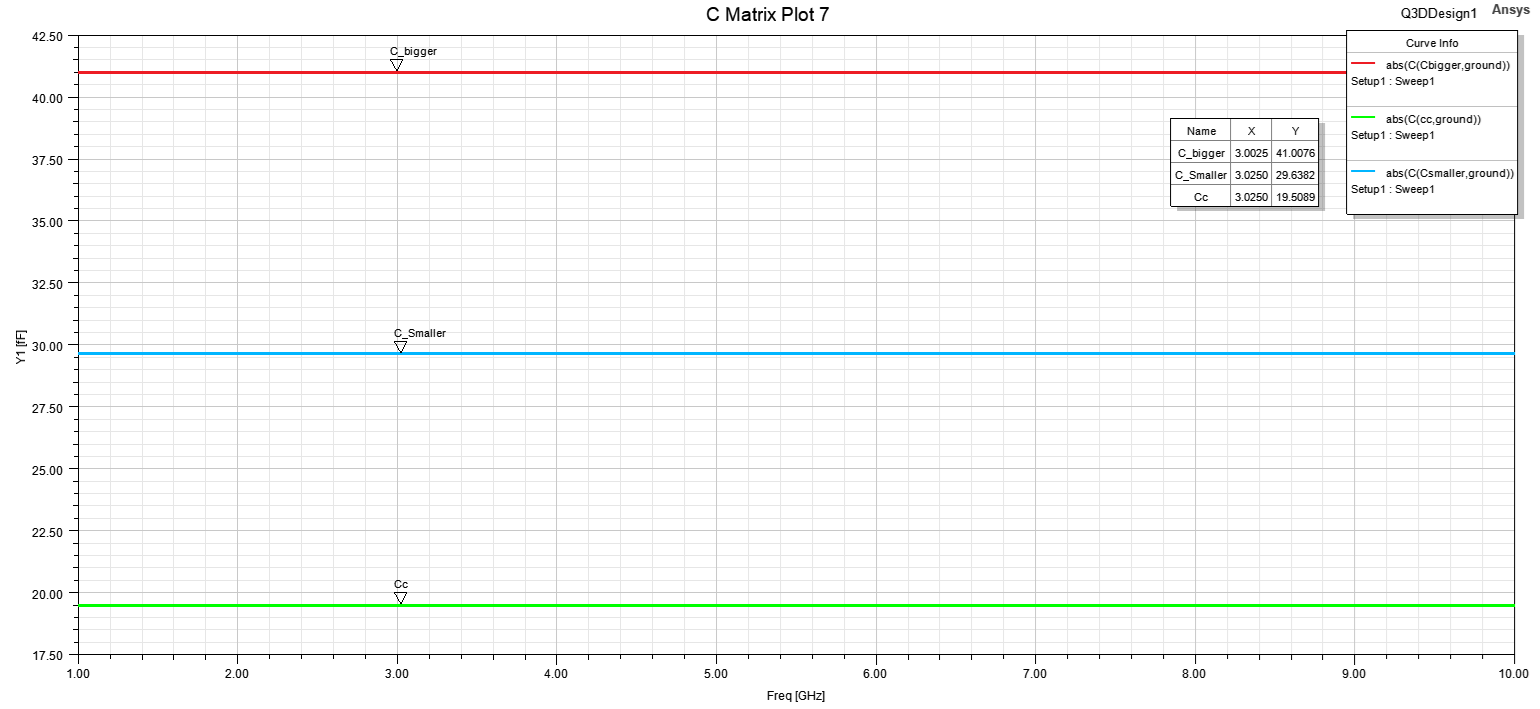
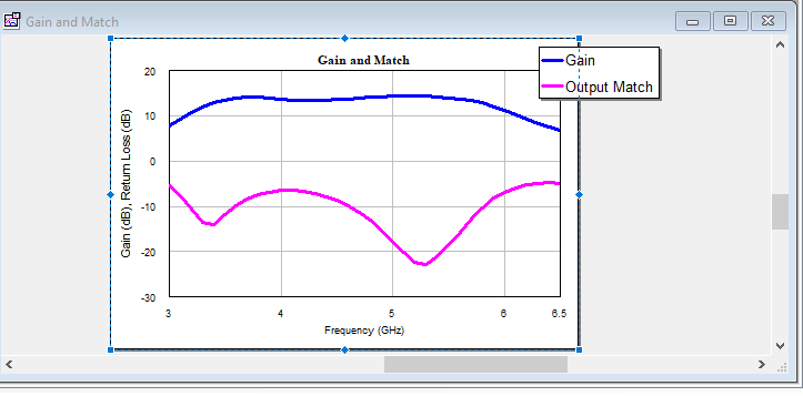
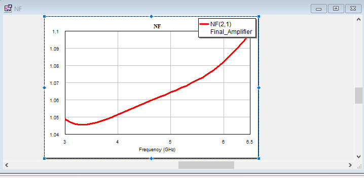
FEM and circuit simulations. I have prefered softwares, but I can do stuff with various tools one open source and one closed source. For circuit simulations I do schematics, S parameters, Z parameters, currents, Gain plots, Smith charts. For FEM simulation I do fields, S parameters and Z parameters, Inductance extraction, capacitive extraction, EPR of substrate and other different types of simulations
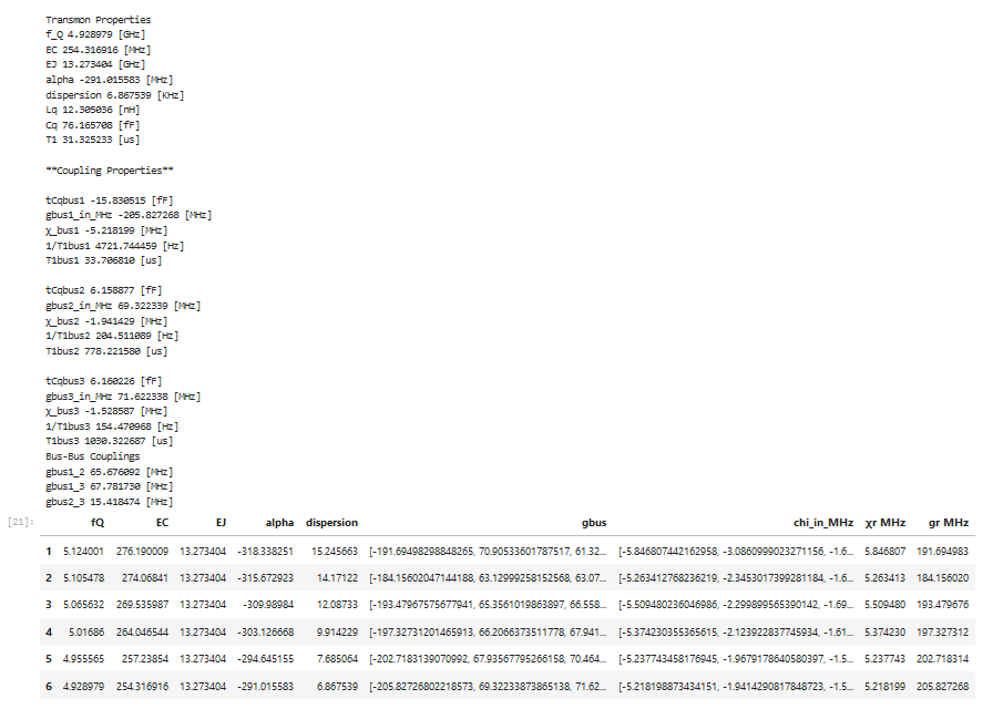
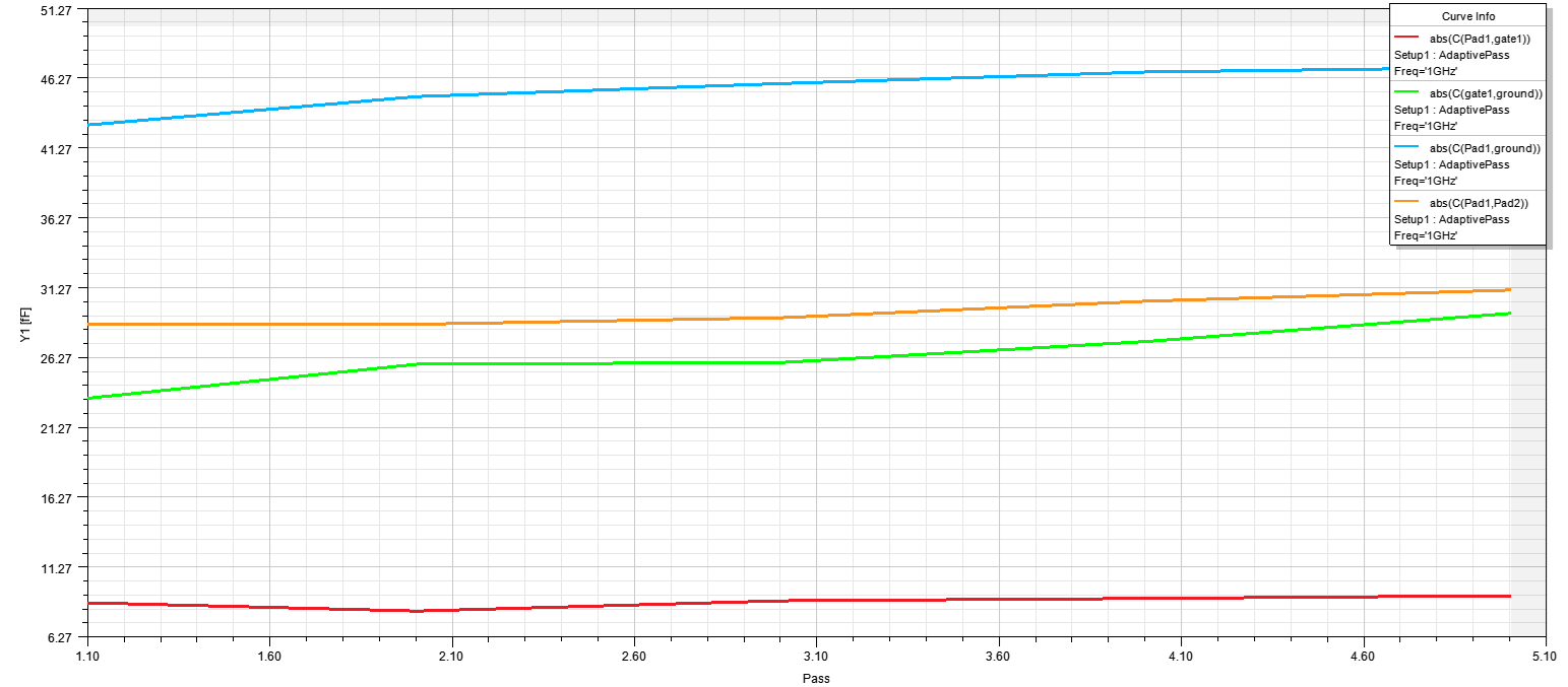
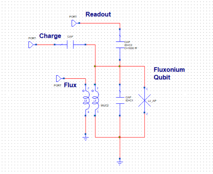
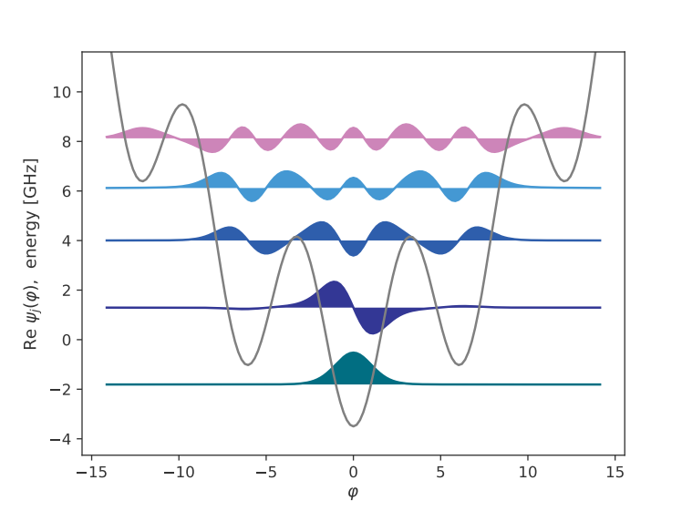
Qubit modelling
Qubit modelling I can design geometry of qubit and import it into qiskit metal. From Circuit simulation I can do S parameters, Z parameters, Current simulations. When This is done I will create layout and import it into qiskit evaluate with circuitry and then do other required post layout simulation in FEM. Like EPR, electric fields, S params, Y params, Capacitance extraction.